
The next step on my Z-80 journey is building the I/O. I decided to do this before building the processor circuit itself as it doubles up as a handy test device.
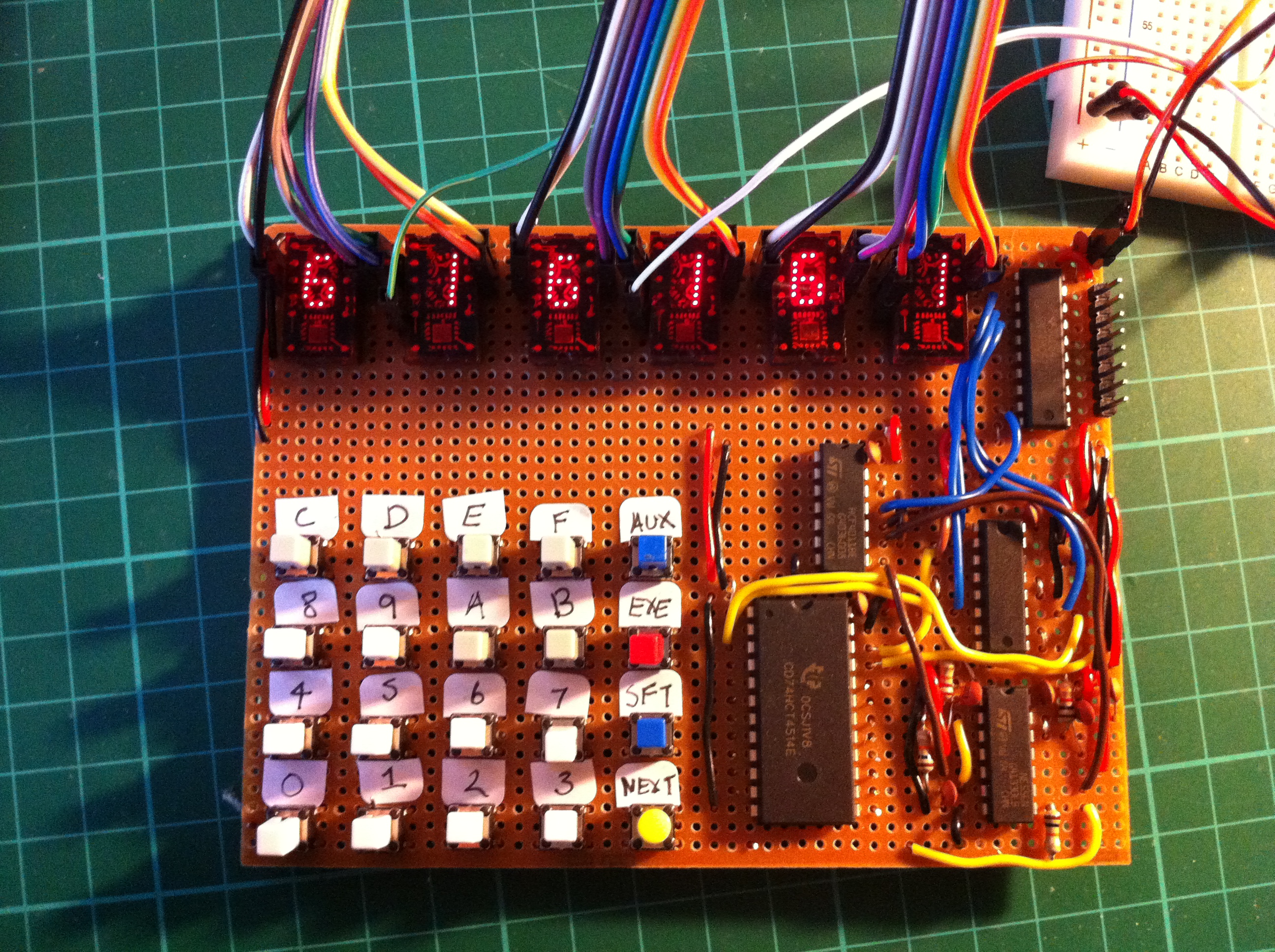
There are three output ports that use TIL311 displays; I got these cheap off eBay from Hong Kong. They take a four-bit input and display it as a hexadecimal value. Therefore, in pairs, they can display binary data from the data bus as a hexadecimal number 00h – FFh. They aren’t all connected to the data bus; I’ve kept them separate, so if necessary I can connect them to the address and data bus and for troubleshooting my ROM programmer.
The keypad follows Ciarcia’s design, but modified to use available components. Basically, there is a 556 timer (lower right chip) that has an astable oscillator providing a clock signal of approx. 3kHz. It goes through a NAND gate (upper left) before driving a binary counter (middle right). The counter outputs a four-bit number to a 4 to 14 demultiplexer (lower left). The 16 outputs are connected to the 16 numerical inputs, which are labelled using handwritten stickers to add to the homebrew feel. When one of these is pressed a monostable timer sends a 10ms signal (longer if the switch is held). First, this debounces the switch; second it stops, via the NAND gate, the clock signal. The four-bit number outputting from the counter is then held at the number pressed, which corresponds to the value of the button, and the four bit number is present at the bus buffer (top right) to be read by the CPU. When the CPU is looking for a value from the keypad it will read this buffer and get the number from the lower four bits. The next three bits are the modifier keys and finally bit 7 is the output from the monostable timer that tells the CPU that a key has been pressed and a value can be read. A software flag will ensure that the value is only read once.
ROM is necessary to boot the computer. Gone, however, are the days of needing EEPROM or UV erasable chips and their expensive programmers. Instead a few pounds will by a 4Mbit CMOS flash chip. So to program this chip, which can be done quickly using a single 5V supply, a simple Arduino sketch is required that uses shift registers to provide a parallel output. This is currently underway and it is possible to debug it using the I/O board.
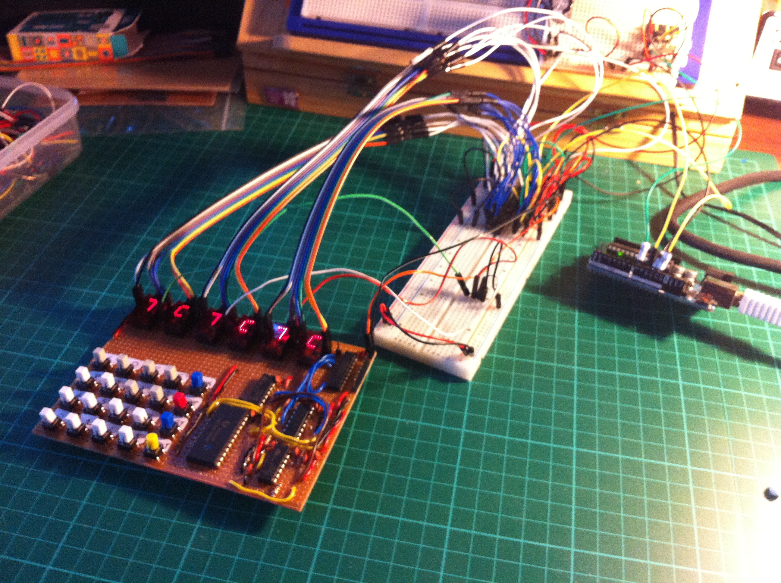
Here, three shift registers are connected to the Arduino providing 8 bytes of output. The top two will drive the address bus and the lower provide the data. For now, though, it is just a proof of concept and is running a simple counter. Eventually, it will be possible to program it using data sent over the serial port of the computer.